
Optical Emission in Semiconductor Materials
Optical Emission in Semiconductor Materials
Optical Emission in Semiconductor Materials
Fundamental radiation processes that occur within semiconductor materials are shown in Figure 1. It also shows the response of a biased p-n junction diode for each process. Absorption produces electron-hole pairs and is the fundamental process exploited in semiconductor photodiodes where the junction is typically reverse biased. In contrast, electroluminescence (or electron-hole recombination radiation following electrical injection) occurs when a p-n junction is forward biased. This radiation is equivalent to spontaneous emission and leads to optical emission in an LED. This recombination radiation can also generate stimulated emission and, if the gain produced in the junction can overcome the optical losses (including absorption), lasing will occur in a laser diode. The evolution of this emission as a function of injection current, the mechanisms for efficient light extraction, and the typical device geometries employed for both LEDs and laser diodes are the subjects of this section.
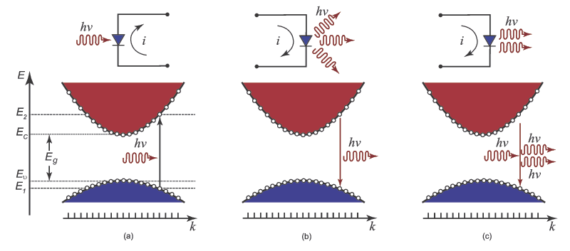
Figure 1. Fundamental radiation processes that occur within a semiconductor p-n junction. Generation of an electron-hole pair by absorption (a) governs the operation of a photodiode. Electron-hole recombination processes give rise to spontaneous emission (b) in an LED and stimulated emission (c) in a laser diode.
Light-Current Curve

Equation 1. Steady-state output power as a function of the current applied to a laser diode.
This relationship is observed in the form of a light-current (L-I) curve in Figure 2. The current value at which the line intersects the x-axis and produces zero emission is the threshold current for lasing (it). The slope of this curve above threshold is known as the differential responsivity (Rd) and is typically expressed in units of W/A or mW/mA. This differential responsivity is determined by the external differential quantum efficiency (ηd), which essentially describes how efficient the laser system is in converting injected electrons into output photons. The efficiency is made up of an internal quantum efficiency (ηi), which is the ratio of generated photons (inside the junction) to injected electrons, and an extraction efficiency (ηe), which is associated with external losses (see section on extraction of light below). Equation (7) can be put in context with the generalized discussion of laser gain from Critical Laser Components where gain was given as the product of the population difference (ΔN) and the transition cross section (σ). ΔN is essentially i divided by the volume of the junction (V) while ηi plays the role of the σ. ηe accounts for the losses associated with the resonator cavity. Interestingly, i/V can also be expressed as a current density J divided by the thickness of the active region (l). In Laser Diode and LED Physics, this reciprocal relationship between J and l was used to explain the benefit of moving from homojunction lasers to DH and QW devices.
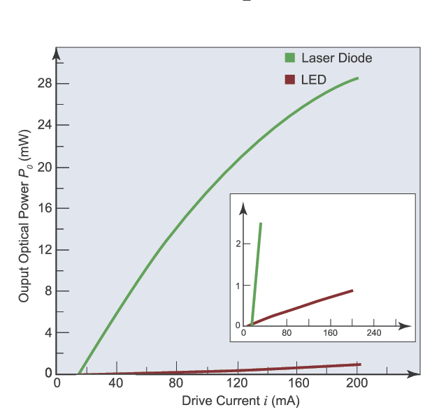
Figure 2. Representative L-I curves for an LED and laser diode operating at a wavelength of 1.6 µm consisting of lnGaAsP / InP multiple QW structures. The inset provides an expanded view.
Equation (1) can also be used to describe the LED output power by setting it = 0 (since there is no threshold for spontaneous emission) Rd and ηd are replaced by the responsivity (R) and the external efficiency (ηex). Figure 2 shows a L-I curve for an LED and laser diode. Despite having the same architectures, the slope of the laser diode curve is significantly higher, indicating a larger value of d compared to . As detailed below, this superior performance is the result of a greater extraction efficiency for the laser diode. A laser diode exhibits the same response as an LED when it is operating below threshold; that is, it emits light spontaneously that propagates in all directions. However, when the laser reaches threshold, stimulated emission concentrates the light into a select number of spatial modes, giving rise to the sharp increase in the observed output power.
The overall efficiency of an LED (ηex) is given by the product of ηi and ηe. While this device may be highly efficient at generating light within the semiconductor material, i.e., ηi approaching unity, the usefulness of the light source is predicated on efficiently extracting light from within the junction to outside the device. Spontaneous emission is isotropic, which implies that the photons generated in the junction of an LED are radiated uniformly in all directions. However, as shown in Figure 3, only a fraction of this light will emerge from an LED with a planar surface. In addition to losses associated with absorption in the material, the large refractive index of the semiconductor (typically between 2.9 and 3.6) gives rise to losses from Fresnel reflections and from total internal reflection (TIR). The latter is particularly detrimental since any light outside of a cone defined by TIR (called the extraction cone) is not transmitted. Depending on the device design and junction geometry, virtually all the light can be either reflected or absorbed, yielding an extraction efficiency of less than 2%. Numerous mitigation approaches are used to enhance ηe. One approach employs an epoxy material formed into a parabolic shape (illustrated in Figure 3), which exploits index-matching and geometry to reduce the impact of reflection losses. Transparent contacts and substrates are used to reduce absorption losses while imparting a texture to a surface can minimize impacts due to TIR. Another way to increase ηe is by incorporating a microresonator that confines light within a very small spatial region. This also creates angular confinement of the light such that it lies within the extraction cone.
Extraction of Light
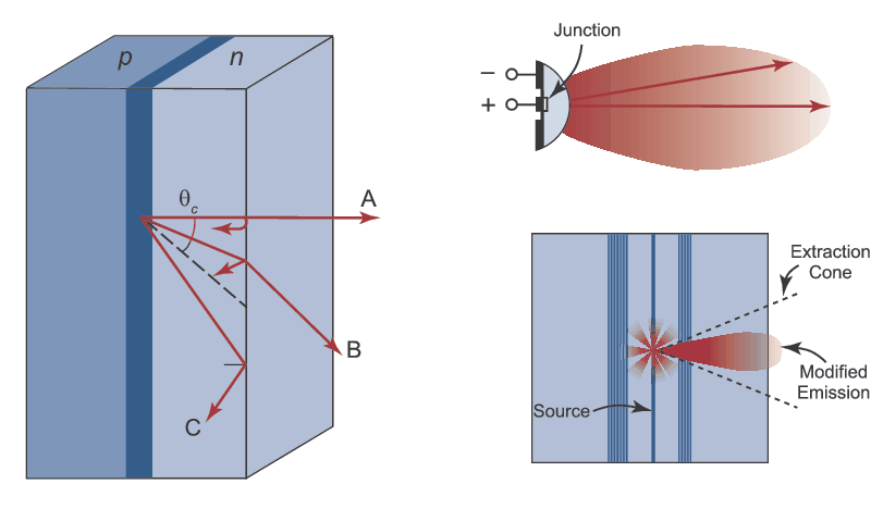
Figure 3. Optical emission from a surface-emitting LED (left) where light rays experience absorption and reflection (both A and B) while those outside of the critical angle undergo TIR (C) and are not extracted. Two methods for increased light extraction are shown on the right, including the use of a parabolic lens made of epoxy (upper right) and a microresonator that narrows the confinement into the light extraction cone (lower right).
In Required Components for Lasing, the laser cavity end mirrors were a source of transmission loss. Since this loss represents useful laser light, the extraction efficiency in a laser diode is defined by the ratio of this loss to the total resonator loss. In this way, if the only losses are associated with laser light exiting the resonator mirror, the system would be considered highly efficient. Other loss sources include optical scattering from any element within the cavity, absorption due to impurities or charge carriers, as well as optical energy that lies outside the active region. Methods for addressing this optical confinement in different laser diode geometries are discussed below.
Semiconductor-based LEDs and laser diodes generally have two emission configurations: edge-emitting, where light exits from the edge of the active region of the device, or surface-emitting, where emission occurs through a face parallel to the plane of the active region. This section will focus on the configurations for laser diodes (see Figure 4). The objective of laser diode design is to minimize the threshold injection current, which is accomplished by reducing the dimensions of the active region. In the direction of the layers, this is achieved using DH or QW architectures. The means for lateral confinement (in the plane of the junction) as well as the method for creating the resonator cavity are specific to the emission configuration. Details regarding edge-emitting lasers will be discussed first. These lasers produce a beam in the plane of the junction region and two methods are used to determine the lateral confinement of the gain. The first method, referred to as gain-guiding, uses fabrication techniques to limit the lateral extent of the gain, e.g., a narrow electrical contact that minimizes the region where current flows. The second method uses index-guiding, where a change in the index of refraction in the lateral direction creates optical confinement in the form of a waveguide. The laser cavity in an edge-emitting laser can be produced in one of two ways. The first way is by cleaving the semiconductor crystal normal to the plane of the junction. The large refractive index of the semiconductor allows these surfaces to function as mirrors with sufficient reflectivity (~ 30%) to create an etalon. In this way, the length of the active region of the p-n junction becomes the resonator length. Figure 4 shows an edge-emitting laser diode with a DH architecture that utilizes gain-guiding for lateral confinement and an etalon structure for feedback. The second type of cavity uses fabrication techniques to produce distributed feedback (DFB) within the crystal or to create distributed Bragg reflector (DBR) structures at the ends of the crystal.
Edge-Emitting and Surface-Emitting
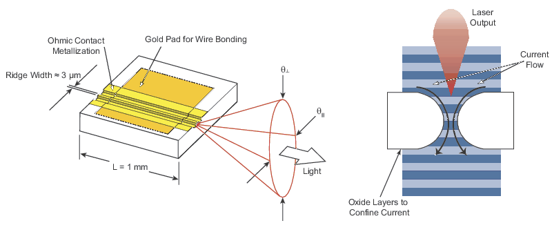
Figure 4. Typical structure and optical emission from an edge-emitting laser diode (left) and a surface-emitting laser diode (right).
Surface-emitting lasers produce a beam in a direction perpendicular to the junction region. A commonly-employed structure is known as a vertical cavity surface emitting laser (VCSEL). Here, mirrors in the form of DBRs clad the active layer which results in a vertical cavity giving rise to a beam that propagates normal to the junction plane. Since the length of the gain medium is defined by the thickness of the active region, much smaller gains are involved compared to edge-emitting lasers. As a result, mirror reflectivities must be very high. Lateral confinement of the gain region is accomplished using dielectric materials which narrow the cross-sectional area of current flow (see Figure 4). The lower optical gain for VCSELs generally results in lower output powers compared to edge-emitting lasers. However, their monolithic construction allows for high packing density of two-dimensional arrays and provides important practical advantages over their edge-emitting counterparts.
Related Topics
Lasers
- Basic Light-Matter Interactions in Lasers
- Required Components for Lasing
- Characteristics of Laser Output
- Types of Lasers
- Methods for Pulsed-Laser Operation
- Spectral Tunability
- Classes of Lasers, Laser Safety, and Laser Damage
Laser Diodes and LEDs