Photodiode Sensor Physics
Photodiode Sensor Physics
Photodiode Sensor Physics

Photodiode Optical Sensors
A photodiode sensor consists of a semiconductor p-n junction like the laser diode and led described in Laser Diode and LED Physics. Light falling on the junction causes the formation of electron-hole pairs. In photovoltaic mode, i.e., no applied bias, the electron-hole pairs migrate to opposite sides of the junction, thus producing a voltage (and a current, if the device is connected in a circuit). However, most photodiodes are operated in the photoconductive mode where a reverse bias is applied across the junction. Operating in this mode offers a few significant advantages. A reverse bias increases the width of the depletion region, which leads to a larger photosensitive area allowing more light collection. Furthermore, the bias produces a strong field in the junction that sweeps the carriers out quickly, making it less likely for recombination to occur. This ensures a large quantum yield or efficient conversion of photons to charge carriers. There are also advantages in terms of response time (see Photoreceiver Physics). In reverse bias photodiodes, the current produced by the bias and charge carriers is proportional to the incident optical intensity over a wide dynamic range.
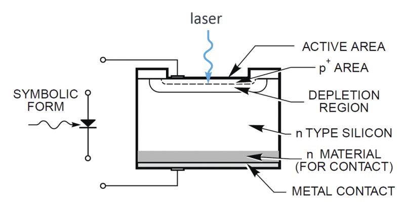
One critical difference between a semiconductor photon source and a photon detector is that the former requires the use of a direct-gap semiconductor while the latter can utilize an indirect-gap semiconductor. While the simultaneous requirement for energy and momentum conservation makes photon emission much less likely in indirect-gap semiconductors, this is not the case for absorption. A readily-achievable two-step process occurs where an electron is excited to a high level in the conduction band followed by a relaxation process where its momentum is transferred to phonons. Since this process can be sequential, it is much more likely than an emission process where the two steps must occur simultaneously. A consequence of this is that Group IV elemental semiconductors such as Si and Germanium (Ge) can be efficient photon detectors similar to direct-gap III-V systems like GaAs or InGaAs. The ubiquitous presence of Si in electronic circuits and devices makes it unsurprising that Si photodiodes are the most common detectors of light used in instrumentation (see Figure 1 for a typical device architecture). The spectral responsivity of Si covers the UV, VIS, and the NIR. Coverage in other portions of the electromagnetic spectrum are possible with photodiodes of other semiconductor materials.
Photodiodes possess several characteristics that set them apart from their thermal counterparts. The conversion of photons to electrons is very rapid and so these detectors have the potential of following fast changing radiation levels. Detectivity can be significantly higher than that of thermal detectors. The detection mechanism is strongly wavelength-dependent, i.e., there is a peak in responsivity that falls off at short wavelengths due to photon-to-watt conversion and at long wavelengths because of the minimum photon energy required to generate electron-hole pairs. The dynamic range of photodiodes can be extremely large, exceeding values of 1010 with a single detector. Due to this large detectivity and dynamic range, photodiodes are often used to measure optical power over a wide range. For CW or quasi-CW sources, this is straightforward and for pulsed sources procedures can be used to estimate pulse energy. Photodiodes can be used as energy sensors as well, provided their temporal response can accommodate the pulse integration. This leads to a reduction in the dynamic range due to decreased detectivity (owing to the faster temporal response) on the low end and due to saturation of the linear response of the detector on the high end. This is because electron-hole pairs begin to recombine instead of flowing through the circuit.

Related Topics
Optical Sensors
Beam Characterization